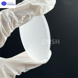
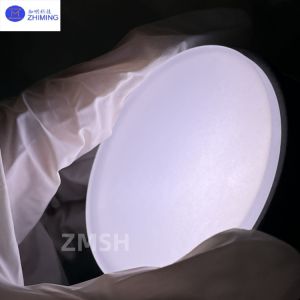
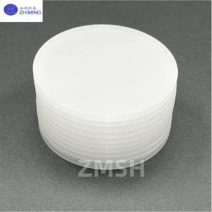
Sapphire Wafer Precision Cutting Diameter 60mm Thickness 3mm
Optical Infrared Window
Sapphire wafer is a precision optical component fabricated from
high-purity aluminum oxide (Al₂O₃) single-crystal material, with
specifications of 60mm in diameter and 3mm in thickness. It achieves high-precision dimensional control through directional
cutting techniques (e.g., laser cutting or diamond wire sawing),
with surface roughness controlled to <0.5μm. The crystal orientation options include C-plane (<0001>),
A-plane (0001), and M-plane (10-10), catering to diverse
application requirements. Inheriting the inherent advantages of sapphire, sapphire wafer
ardness (Mohs hardness of 9), high-temperature resistance (melting
point of 2045°C), low thermal expansion coefficient (5.3×10⁻⁷/°C),
and broad-spectrum transparency (0.15–5.5μm), making it a core
material for advanced optoelectronics, semiconductors, and
precision instrumentation.


Sapphire Wafer Technical Parameter
Parameter
| This Product (60mm×3mm)
|
Thermal Conductivity
| 42 W/m·K
|
Bending Strength
| 350 MPa
|
Transmittance (400nm)
| >85%
|
Temperature Range
| -200–1600°C
|
Cost per Piece (CNY)
| 800–1200
|
(Data based on C-plane cutting and double-sided polishing.
Customizable parameters available.)
|
Sapphire Wafer Key Features & Advantages
1. Extreme Environmental Adaptability
- Sapphire wafer maintains stability under high temperatures
(>300°C), strong acids/alkalis, and high-vacuum environments.
Suitable for aerospace sensors, laser windows, and other harsh
scenarios. Exhibits outstanding thermal shock resistance (withstand
temperature differentials >1000°C) without cracking.
2. Superior Optical Performance
- High Transmittance: Sapphire wafer with >85% in visible
light (400–700nm) and >70% in ultraviolet (200–400nm),
outperforming standard glass and quartz.
- Low Absorption: Sapphire wafer with <0.1% absorption in
near-infrared (1–5μm), ideal for infrared imaging and quantum
communication systems.
3. Mechanical & Chemical Stability
- Scratch Resistance: Mohs hardness of 9, 10× more wear-resistant
than quartz, ensuring long-term surface integrity.
- Corrosion Resistance: Withstands all acids/alkalis except
hydrofluoric acid, suitable for marine equipment and chemical
detection instruments.
4. Precision Fabrication
- Achieves ±0.02mm thickness tolerance and ±0.05mm diameter
tolerance, ensuring batch consistency. Offers double-sided
polishing (Ra <0.1nm) or single-sided polishing for tailored
optical designs.


Sapphire Wafer Application Fields

1. Optoelectronic Devices
- LED Substrates: Sapphire wafer serves as gallium nitride (GaN)
epitaxial growth substrates, enhancing LED efficiency (>120
lm/W) and lifespan (>100,000 hours) for high-end lighting and
displays.
- Laser Windows: Sapphire wafer used in high-power lasers (e.g.,
fiber lasers) as input/output mirrors, tolerating >10 MW/cm²
intensity with minimized thermal distortion.
2. Semiconductors & Microelectronics
- Wafer Dicing: Sapphire wafer acts as cutting blade substrates
for semiconductor wafer slicing, reducing edge chipping (<5%)
and improving yield.
- Infrared Sensors: Fabricates 8–12μm infrared detector windows,
Sapphire wafer for security surveillance and industrial temperature
measurement.
3. Precision Optical Systems
- Camera Lenses: Protects smartphone/camera lenses, tripling
impact resistance and reducing weight by 40% at 3mm thickness.
- UV Optical Components: Sapphire wafer enables deep-UV
lithography optics (248nm wavelength) for advanced semiconductor
manufacturing.
4. Defense & Aerospace
- Missile Nose Cones: Sapphire wafer withstands >800°C
temperatures and impacts, safeguarding guidance system optics in
extreme conditions.
- Satellite Thermal Control: Sapphire wafer functions as
radiation heat sink substrates, regulating spacecraft temperature
with ±1°C precision.
5. Emerging Technologies
- Flexible Electronics: Ultra-thin sapphire (3mm) enables
foldable smartphone displays with >100,000 bending cycles.
- Quantum Computing: Sapphire wafer acts as photonic chip
packaging substrates, reducing signal loss (<0.5 dB/cm).
Related product recommendations
1. 12inch Sapphire wafer sapphire substrate Al2O3 wafer 9.0Mohs
transparent SSP DSP C-axis

Sapphire Wafer FAQ
1. Q: What are the key advantages of sapphire wafer cutting discs
(60mm×3mm)?
A: High-temperature resistance (>1600°C), scratch-proof (Mohs 9
hardness), and broad-spectrum transparency (0.15–5.5μm).
2. Q: What’s your MOQ and lead time for customized orders?
A: MOQ starts at 25pcs, standard lead time 2–4 weeks for bulk
production.
Tags: #Sapphire Wafer, #Precision Cutting, #Diameter 60mm, #Thickness 3mm, #Optical Infrared Window


